


扫一扫
关注中图网
官方微博


本类五星书更多>
-
>
中医基础理论

-
>
高校军事课教程
-
>
毛泽东思想和中国特色社会主义理论体系概论(2021年版)
-
>
中医内科学·全国中医药行业高等教育“十四五”规划教材
-
>
中医诊断学--新世纪第五版
-
>
中药学·全国中医药行业高等教育“十四五”规划教材
-
>
中医外科学——全国中医药行业高等教育“十四五”规划教材


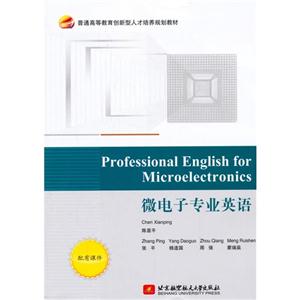
微电子专业英语-配有课件 版权信息
- ISBN:9787512417304
- 条形码:9787512417304 ; 978-7-5124-1730-4
- 装帧:一般胶版纸
- 册数:暂无
- 重量:暂无
- 所属分类:>>
微电子专业英语-配有课件 内容简介
《Professional English for Microelectronics微电子专业英语》较全面、系统地介绍了半导体物理的基本理论、半导体器件原理及MEMS设计的相关知识。主要内容包括:半导体、杂质、能带、晶格等基本概念,二极管的结构、电流、电压特性、开关特性,双极型、MOS晶体管的电流、电压方程、瞬变特性、开关特性、击穿特性及较新的结构设计,同时介绍了MEMS的基本概念、设计方法、应用及未来发展方向。 《Professional English for Microelectronics微电子专业英语》可以作为高等学校微电子、集成电路专业本科生专业英语教材,也可供从事相关领域科研工作的技术人员阅读参考。
微电子专业英语-配有课件 目录
PART I Basic knowledge of semiconductor physics and semiconductor devices Chapter 1 Semiconductor 1.1 Early history of semiconductors 1.2 Properties and materials of semiconductor 1.3 Band theory of solids 1.4 Charge carrier (electrons and holes) 1.4.1 The carrier concentration 1.4.2 Carrier generation and recombination 1.4.3 Drift and diffusion current 1.5 Electrical conduction 1.6 Doping of semiconductor 1.7 Type of semiconductor 1.7.1 N-type semiconductor 1.7.2 P-type semiconductor 1.8 Questions 1.9 References Chapter 2 Semiconductor devices 2.1 PN junction 2.1.1 Basic structure of the PN junction 2.1.2 Unbiased PN junction 2.1.3 The current-voltage characteristic of PN junction 2.1.4 The breakdown of PN junction 2.1.5 Junction capacitance 2.1.6 The applications of PN junction 2.2 Schottky diode 2.2.1 The structure of Schottky diode 2.2.2 The principle of Schottky diode 2.2.3 The characteristics of Schottky diode 2.2.4 The applications of Schottky diode 2.3 Heterojunction diode 2.3.1 The concept of heterojunction 2.3.2 The characteristics of heterojunction diode 2.3.3 The application of heterojunction diode 2.4 Bipolar junction transistor(BJT) 2.4.1 The basic structure of BJT 2.4.2 The current transfer characteristic of transistor 2.4.3 Basic configurations and modes of operation 2.4.4 The application of transistor 2.5 The MOS transistor 2.5.1 The basic structure of MOS transistor 2.5.2 The form of inversion layer of MOSFET 2.5.3 The basic operation and DC characteristic of MOSFET 2.5.4 The types of MOSFET 2.5.5 The terminal capacitances of MOSFET 2.5.6 The advantage and application of MOSFET 2.6 Questions 2.7 ReferencesPART II Manufacturing technologies and processes Chapter 3 Doping technology and hot processing 3.1 Doping 3.1.1 Diffusion 3.1.2 Ion implantation 3.1.3 Idealized ion implantation systems 3.1.4 Channeling effects 3.1.5 Shadowing effects 3.1.6 Ion implantation damage 3.2 Thermal oxidation 3.3 Rapid thermal proeessing(RTP) 3.3.1 RTP configuration and chamber design 3.3.2 Rapid thermal activation of impurities 3.3.3 Rapid thermal processing of dielectrics 3.4 Questions 3.5 References Chapter 4 Pattern transfer 4.1 Photolithography 4.2 Photoresist (PR) 4.2.1 Composition of PR 4.2.2 The types of PR 4.2.3 The contrast curve of PR 4.3 The pre-exposure process 4.3.1 Priming 4.3.2 Photoresist coating 4.3.3 Soft bake 4.4 Alignment and exposure 4.4.1 Printer 4.4.2 Photomask fabrication 4.4.3 Alignment 4.4.4 Exposure 4.5 Postexposure 4.5.1 Postexposure bake 4.5.2 Development 4.5.3 Hard bake 4.5.4 Pattern inspection 4.6 Nonoptical lithographic techniques 4.6.1 X-ray lithography (XRL) 4.6.2 Projection X-ray lithography 4.6.3 Electron beam lithography (EBL) 4.6.4 Projection electron beam lithography (SCALPEL) 4.6.5 Ion beam lithography 4.6.6 EBL and XRL resist 4.7 Etch 4.7.1 Introduction 4.7.2 The characteristic of etch 4.7.3 Wet etch process 4.7.4 Chemical mechanical polishing (CMP) 4.7.5 Dry etching 4.8 High density plasma (HDP) etching 4.9 Liftoff 4.10 Questions 4.11 References Chapter 5 Thin film 5.1 The introduction of thin film 5.1.1 Metallic thin films 5.1.2 Polysilicon 5.1.3 Oxide and nitride thin films 5.2 Physical vapor deposition 5.2.1 Evaporation 5.2.2 Sputter 5.3 Chemical vapor deposition 5.3. 1 Chemical vapor deposition process description 5.3.2 Classification of CVD reactors 5.3.3 Atmospheric pressure CVD 5.3.4 Low pressure CVD in hot wall systems 5.3.5 Plasma-enhanced CVD 5.3.6 Step coverage 5.4 Epitaxial growth 5.4.1 Homoepitaxy 5.4.2 Vapor phase epitaxy 5.4.3 VPE hardware 5.4.4 Epitaxy process 5.4.5 Selective epitaxial growth 5.4.6 Heteroepitaxy 5.4.7 MBE 5.4.8 MOCVD 5.5 Questions 5.6 References Chapter 6 Process Integration 6.1 CMOS 6.1.1 Introduction 6.1.2 The formation of the CMOS process 6.2 Microelectromechanical system (MEMS) 6.2.1 Introduction 6.2.2 The types and advantages of MEMS 6.2.3 The processes of MEMS 6.3 Nanoelectromechanical system (NEMS) 6.4 Questions 6.5 ReferencesPART III Frontiers of science and technology Chapter 7 More than Moore:creating high value micro/ nanoelectronics systems 7.1 Introduction 7.2 Preconditions for an industry-wide technical roadmap 7.3 Lessons learned from "More Moore" 7.3.1 Metallic nanowires 7.3.2 Combining focus and variety 7.4 Proposed methodology for "More-than-Moore" 7.5 Applying the proposed methodology 7.5.1 Form societal needs to markets 7.5.2 MtM devices 7.6 Summary 7.7 ReferencesPART IV Development of professional English ability Chapter 8 How to write a scientific paper 8.1 What is a scientific paper?
8.1.1 The structure of a paper 8.1.2 Steps for writing a paper 8.2 Searching information in databases 8.2.1 Web of Science 8.2.2 Google Scholar 8.3 How to prepare the Title 8.4 How to prepare the abstract 8.5 How to write the Introduction 8.6 How to write the Materials and Methods section 8.7 How to write the Results 8.8 How to write the Discussion 8.9 How to state the Acknowledgment 8.10 How to cite the Reference 8.11 Questions 8.12 References Chapter 9 How to make a successful presentation 9.1 Attention curve 9.2 How to make a great PowerPoint presentation 9.2.1 Create your narrative 9.2.2 Utilize the format 9.3 How to prepare an oral presentation 9.3.1 Before your presentation 9.3.2 During your presentation 9.3.3 Warnings for oral presentation 9.4 Questions 9.5 References
展开全部
书友推荐
- >
上帝之肋:男人的真实旅程

上帝之肋:男人的真实旅程
¥19.3¥35.0 - >
我与地坛
我与地坛
¥16.8¥28.0 - >
罗庸西南联大授课录
罗庸西南联大授课录
¥13.8¥32.0 - >
有舍有得是人生
有舍有得是人生
¥21.2¥45.0 - >
推拿
推拿
¥12.2¥32.0 - >
二体千字文
二体千字文
¥16.0¥40.0 - >
伯纳黛特,你要去哪(2021新版)
伯纳黛特,你要去哪(2021新版)
¥15.9¥49.8 - >
新文学天穹两巨星--鲁迅与胡适/红烛学术丛书(红烛学术丛书)
新文学天穹两巨星--鲁迅与胡适/红烛学术丛书(红烛学术丛书)
¥9.9¥23.0
本类畅销
-

家居设计解剖书
¥27.3¥39 -
网络安全基础
¥27.7¥39.5 -
家具造型设计
¥34.3¥49 -
工程硕士研究生英语基础教程学生用书
¥45.6¥68 -
国外电子与通信教材系列信号与系统(第二版)
¥69.3¥99 -
工程机械维修
¥30.8¥40