


扫一扫
关注中图网
官方微博


本类五星书更多>
-
>
中医基础理论

-
>
高校军事课教程
-
>
毛泽东思想和中国特色社会主义理论体系概论(2021年版)
-
>
中医内科学·全国中医药行业高等教育“十四五”规划教材
-
>
中医诊断学--新世纪第五版
-
>
中药学·全国中医药行业高等教育“十四五”规划教材
-
>
中医外科学——全国中医药行业高等教育“十四五”规划教材


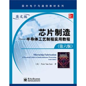
芯片制造-半导体工艺制程实用教程-(第六版) 版权信息
- ISBN:9787121243783
- 条形码:9787121243783 ; 978-7-121-24378-3
- 装帧:一般胶版纸
- 册数:暂无
- 重量:暂无
- 所属分类:>>
芯片制造-半导体工艺制程实用教程-(第六版) 本书特色
本书是一本介绍半导体集成电路和器件制造技术的专业书籍,在半导体领域享有很高的声誉。本书的范围包括半导体工艺的每个阶段:从原材料的制备到封装、测试和成品运输,以及传统的和现代的工艺。全书提供了详细的插图和实例,每章包含回顾总结和习题,并辅以丰富的术语表。第六版修订了微芯片制造领域的新进展,讨论了用于图形化、掺杂和薄膜步骤的先进工艺和尖端技术,使隐含在复杂的现代半导体制造材料和工艺中的物理、化学和电子的基础知识更易理解。本书的主要特点是避开了复杂的数学问题介绍工艺技术内容;加入了半导体业界的新成果,可以使读者了解工艺技术发展的趋势。
芯片制造-半导体工艺制程实用教程-(第六版) 内容简介
半导体集成电路和器件制造技术权威著作,涉及半导体工艺的每个阶段和*新技术发展。
芯片制造-半导体工艺制程实用教程-(第六版) 目录
1 the semiconductor industry
introduction
birth of an industry
the solid-state era
integrated circuits (ics)
process and product trends
moore’s law
decreasing feature size
increasing chip and wafer size
reduction in defect density
increase in interconnection levels
the semiconductor industry association roadmap
chip cost
industry organization
stages of manufacturing
six decades of advances in microchip fabrication processes
the nano era
review topics
references
2 properties of semiconductor materials and chemicals
introduction
atomic structure
the bohr atom
the periodic table of the elements
electrical conduction
conductors
dielectrics and capacitors
resistors
intrinsic semiconductors
doped semiconductors
electron and hole conduction
carrier mobility
semiconductor production materials
germanium and silicon
semiconducting compounds
silicon germanium
engineered substrates
ferroelectric materials
diamond semiconductors
process chemicals
molecules, compounds, and mixtures
ions
states of matter
solids, liquids, and gases
plasma state
properties of matter
temperature
density, specic gravity, and vapor density
pressure and vacuum
acids, alkalis, and solvents
acids and alkalis
solvents
chemical purity and cleanliness
safety issues
the material safety data sheet
review topics
references
3 crystal growth and silicon wafer preparation
introduction
semiconductor silicon preparation
silicon wafer preparation stages
crystalline materials
unit cells
poly and single crystals
crystal orientation
crystal growth
czochralski method
liquid-encapsulated czochralski
float zone
crystal and wafer quality
point defects
dislocations
growth defects
wafer preparation
end cropping
diameter grinding
crystal orientation, conductivity, and resistivity check
grinding orientation indicators
wafer slicing
wafer marking
rough polish
chemical mechanical polishing
backside processing
double-sided polishing
edge grinding and polishing
wafer evaluation
oxidation
packaging
wafer types and uses
reclaim wafers
engineered wafers (substrates)
review topics
references
4 overview of wafer fabrication and packaging
introduction
goal of wafer fabrication
wafer terminology
chip terminology
basic wafer-fabrication operations
layering
patterning
circuit design
reticle and masks
doping
heat treatments
example fabrication process
wafer sort
packaging
summary
review topics
references
5 contamination control
introduction
the problem
contamination-caused problems
contamination sources
general sources
air
clean air strategies
cleanroom workstation strategy
tunnel or bay concept
micro- and mini-environments
temperature, humidity, and smog
cleanroom construction
construction materials
cleanroom elements
personnel-generated contamination
process water
process chemicals
equipment
cleanroom materials and supplies
cleanroom maintenance
wafer-surface cleaning
particulate removal
wafer scrubbers
high-pressure water cleaning
organic residues
inorganic residues
chemical-cleaning solutions
general chemical cleaning
oxide layer removal
room temperature and ozonated chemistries
water rinsing
drying techniques
contamination detection
review topics
references
6 productivity and process yields
overview
yield measurement points
accumulative wafer-fabrication yield
wafer-fabrication yield limiters
number of process steps
wafer breakage and warping
process variation
mask defects
wafer-sort yield factors
wafer diameter and edge die
wafer diameter and die size
展开全部
芯片制造-半导体工艺制程实用教程-(第六版) 作者简介
Peter Van Zant 国际知名半导体专家,具有广阔的工艺工程、培训、咨询和写作方面的背景。他曾先后在IBM和德州仪器(TI)工作,之后在硅谷,又先后在美国国家半导体(National Semiconductor)和单片存储器(Monolithic Memories)公司任晶圆制造工艺工程和管理职位。他还曾在加利福尼亚州洛杉矶的山麓学院(Foothill College)任讲师,讲授半导体课程和针对初始工艺工程师的高级课程。
书友推荐
- >
月亮与六便士
月亮与六便士
¥13.4¥42.0 - >
中国历史的瞬间
中国历史的瞬间
¥19.0¥38.0 - >
中国人在乌苏里边疆区:历史与人类学概述
中国人在乌苏里边疆区:历史与人类学概述
¥24.0¥48.0 - >
诗经-先民的歌唱
诗经-先民的歌唱
¥15.1¥39.8 - >
上帝之肋:男人的真实旅程
上帝之肋:男人的真实旅程
¥19.3¥35.0 - >
巴金-再思录
巴金-再思录
¥33.1¥46.0 - >
名家带你读鲁迅:朝花夕拾
名家带你读鲁迅:朝花夕拾
¥10.5¥21.0 - >
伊索寓言-世界文学名著典藏-全译本
伊索寓言-世界文学名著典藏-全译本
¥6.1¥19.0
本类畅销
-

家居设计解剖书
¥27.3¥39 -
网络安全基础
¥27.7¥39.5 -
家具造型设计
¥34.3¥49 -
工程硕士研究生英语基础教程学生用书
¥45.6¥68 -
国外电子与通信教材系列信号与系统(第二版)
¥69.3¥99 -
工程机械维修
¥30.8¥40